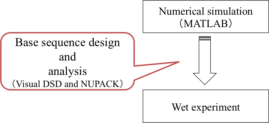
We used Visual DSD and NUPACK in designing DNA sequences for our wet experiments.
Visual DSD is a software which simulates and analyzes DNA strand displacement reactions, and can be utilized as a programing language for a computer-aided design of DNA circuits. With this language, some basic elements such as sequence domains, toeholds, and branch migration are defined, and automatically connected according to their complementation through the compile process. In other words, we can easily create a DNA reaction system by just preparing single- and double-stranded DNAs. In simulating the DNA circuit designed, deterministic or stochastic simulator is available to the designer’s needs in which the former solves an ordinary differential equations of the system, and the latter provides a possible trajectory of the system. It should be noted that Visual DSD can not deal with any DNA secondary structure.
First, we have accomplished the operation check of the three-bit A/D converter in numerical simulation with MATLAB. Second, by using Visual DSD, we have confirmed whether the three-bit A/D converter is feasible in wet experiments. At the same time, this step provides a clue to appropriately design base sequences to be needed in wet experiments. Therefore, simulations in Visual DSD is an important process that connects between numerical simulations and wet experiments. ossible trajectory of the system. It should be noted that Visual DSD can not deal with any DNA secondary structure.
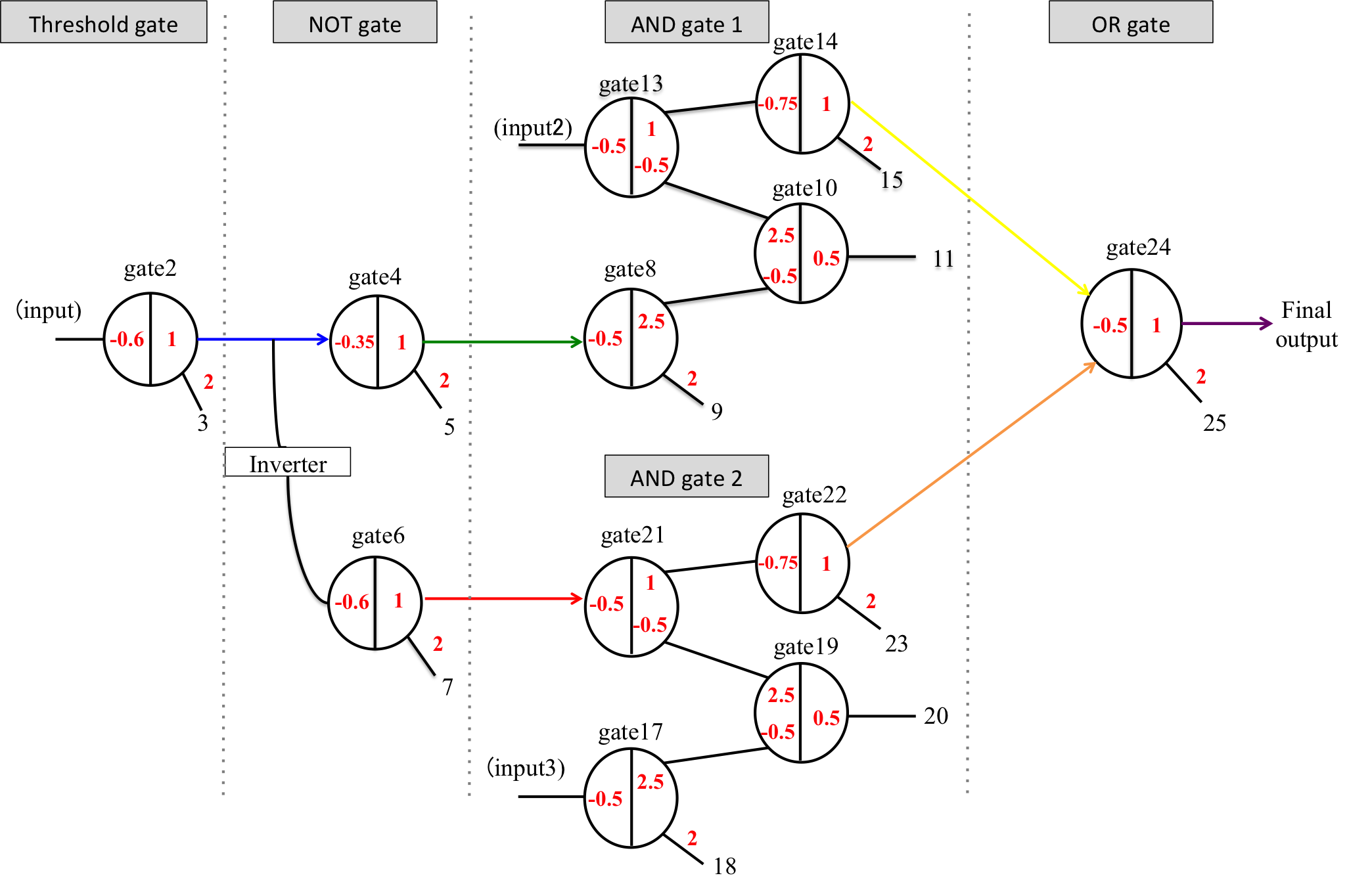
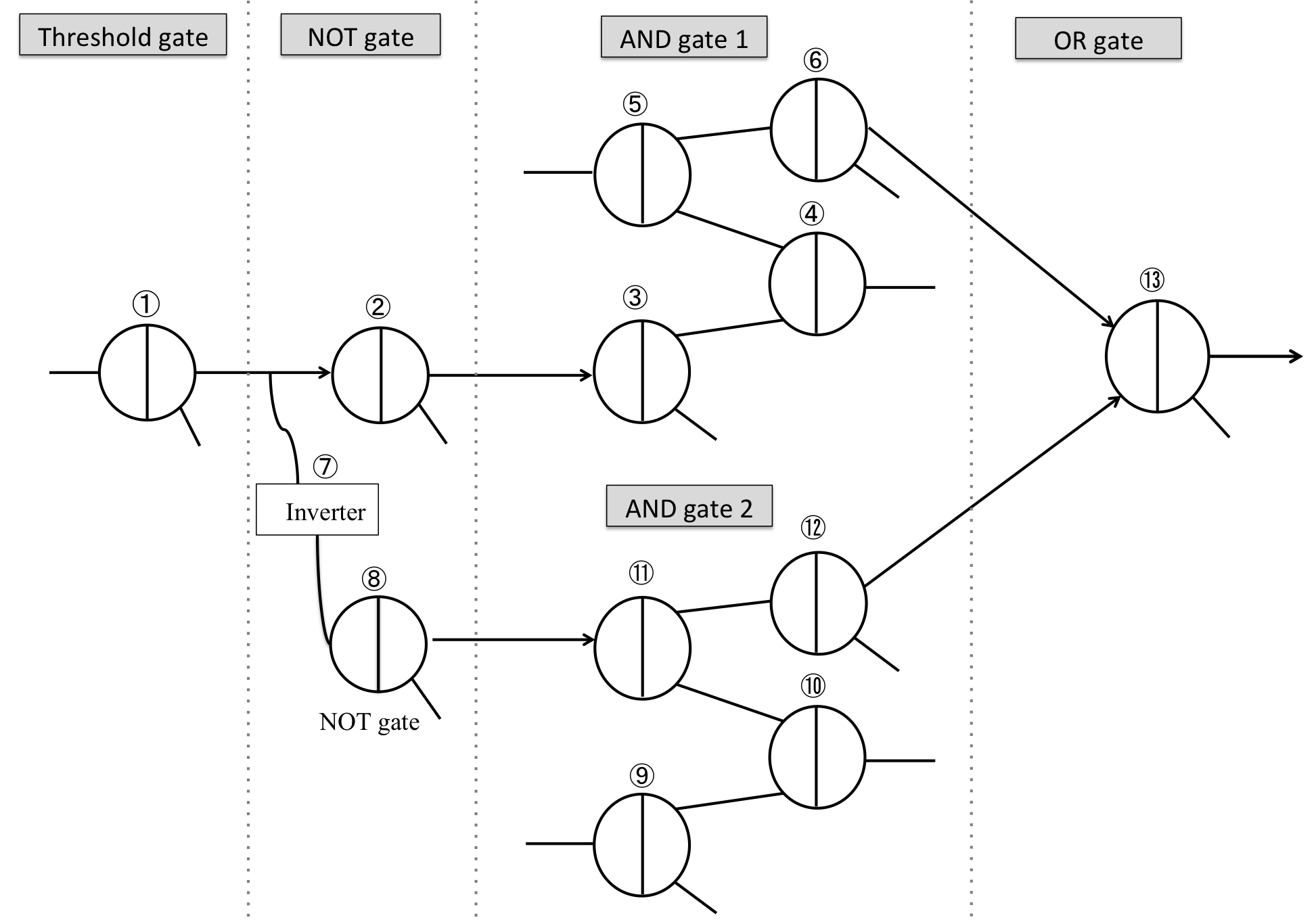
Wet experiments as a verification study should be simply designed. In our case, the essential element of the three-bit A/D converter can be checked by using one-bit A/D converter because three-bit A/D converter can be straightforward made by combining “three” one-bit A/D converters. Figure 2 shows the schematic of one-bit A/D converter in which the system is comprised of four kinds of DNA gates (Threshold, NOT, AND, and OR gates). After preparing all of the gates in Visual DSD, they are integrated into a whole system.
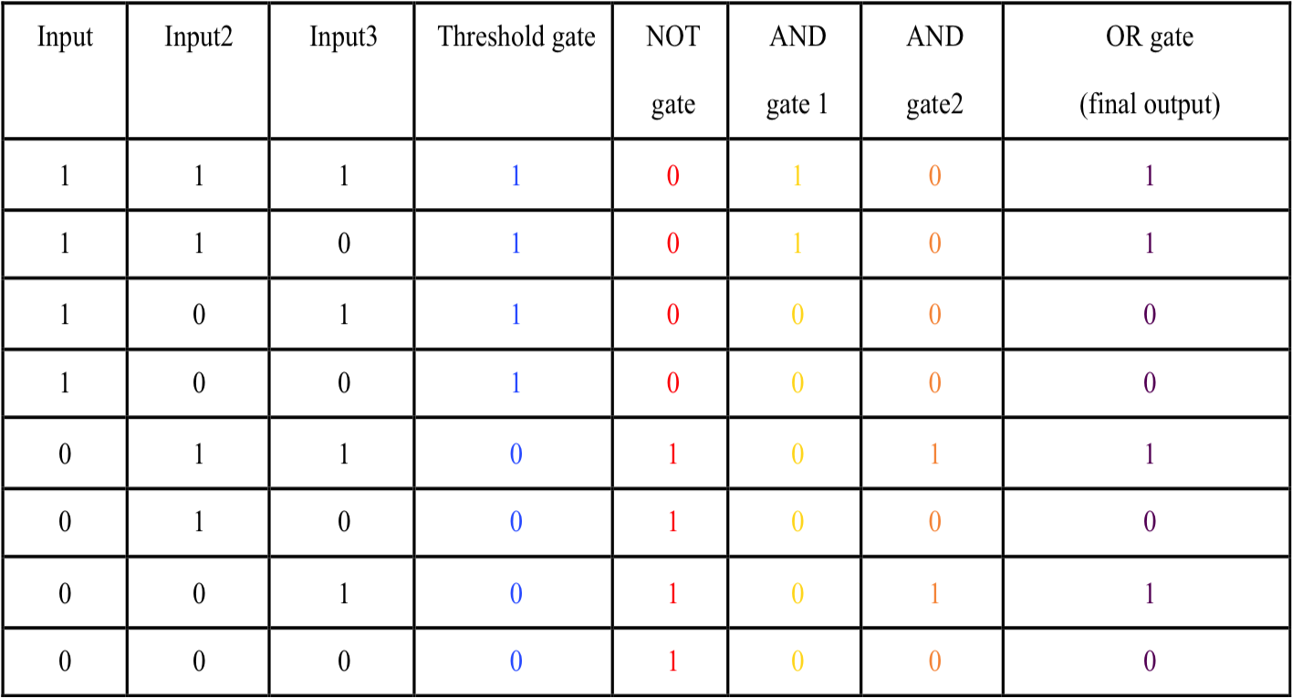
The following Table shows the truth table of the one-bit A/D converter to be checked.
In what follows, we summarize the stochastic simulation results of the one-bit A/D converter with Visual DSD in which
i)The threshold for determining “high” or ”low” is set to 0.5 nM, and we show the threshold value as black line. This means, the output from each gate is defined as high when it exceed the black line. Conversely, we defined outputs of less than black line, as low.
ⅱ)The output from each gate is labeled and colored as follows:
output from gate2 of Threshold gate (blue line) <s4 T s2>
output from gate4 of NOT gate(green line) <s8 T s2>
output from gate6 of NOT gate (red line) <s21 T s6>
output from gate14 of AND gate1 (yellow line) <s24 T s14>
output from gate22 of AND gate2 (orange line) <s24 T s22>
output from gate24 of OR gate (purple line) <s26 T s24>
First of all, we show the simulation results for simple threshold gate in Figure 3.
.png)
.png)
Figure 3: Simulation results for simple threshold gate and input concentrations of 0.8 nM(left),input concentration of 0.2nM(right).
As show in Figure 3, we confirmed the validity of simple threshold gate. Next, we simulated one-bit A/D converter.
1) Input,Input2,Input3 … 1 1 1
(blue line) <s4 T s2>… high
(green line) <s8 T s2>… high
(red line) <s21 T s6>… low
(yellow line) <s24 T s14>… high
(orange line) <s24 T s22>… low
(purple line) <s26 T s24>… high
.png)
2) Input,Input2,Input3 … 1 1 0
(blue line) <s4 T s2>… high
(green line) <s8 T s2>… high
(red line) <s21 T s6>… low
(yellow line) <s24 T s14>… high
(orange line) <s24 T s22>… low
(purple line) <s26 T s24>… high
.png)
3) Input,Input2,Input3 … 1 0 1
(blue line) <s4 T s2>… high
(green line) <s8 T s2>… high
(red line) <s21 T s6>… low
(yellow line) <s24 T s14>… low
(orange line) <s24 T s22>… low
(purple line) <s26 T s24>… low
.png)
4) Input,Input2,Input3 … 1 0 0
(blue line) <s4 T s2>… high
(green line) <s8 T s2>… high
(red line) <s21 T s6>… low
(yellow line) <s24 T s14>… low
(orange line) <s24 T s22>… low
(purple line) <s26 T s24>… low
.png)
5) Input,Input2,Input3 … 0 1 1
(blue line) <s4 T s2>… low
(green line) <s8 T s2>… low
(red line) <s21 T s6>… high
(yellow line) <s24 T s14>… low
(orange line) <s24 T s22>… high
(purple line) <s26 T s24>… high
.png)
6) Input,Input2,Input3 … 0 1 0
(blue line) <s4 T s2>… low
(green line) <s8 T s2>… low
(red line) <s21 T s6>… high
(yellow line) <s24 T s14>… low
(orange line) <s24 T s22>… low
(purple line) <s26 T s24>… low
.png)
7) Input,Input2,Input3 … 0 0 1
(blue line) <s4 T s2>… low
(green line) <s8 T s2>… low
(red line) <s21 T s6>… low
(yellow line) <s24 T s14>… low
(orange line) <s24 T s22>… high
(purple line) <s26 T s24>… high
.png)
8) Input,Input2,Input3 … 0 0 0
(blue line) <s4 T s2>… low
(green line) <s8 T s2>… low
(red line) <s21 T s6>… low
(yellow line) <s24 T s14>… low
(orange line) <s24 T s22>… low
(purple line) <s26 T s24>… low
.png)
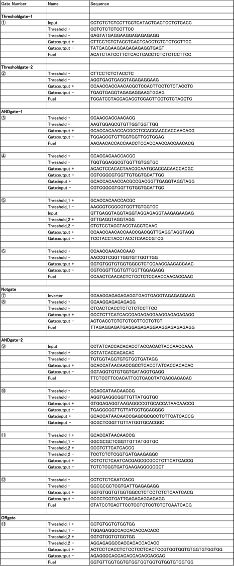
FigureX shows the schematic of Threshold gate. It needs four kinds of DNA strands (Input, Threshold, Gate:output, Fuel). Because NUPACK cannot deal with a double-strand DNA, Threshold and Gate:output are evaluated dividing them into two single-stranded DNAs in which each domain is labeled as follows:
S1=15, S1*=3, S2=15, S2*=15, T1=5, T1*=5, T2=5, T2*=5
We checked the secondary structures for all DNA sequences and calculated the minimum free energy of all combinations (pairs) of DNA sequences.